Category: News Circuit


GOING THE NANO WAY!

Part 1:

By Chetana Deshpande.

The field of nanotechnology has, over the last decade, been surrounded by enormous amount of hype. Therefore, it is almost a compulsion to have at least minimal knowledge about this exciting field. Nanotechnology is simply the study of manipulating matter at the nanoscale, i.e., 1-100 nanometers (nm). It focuses on understanding, controlling and exploiting the properties of materials or structures in the nanoscale. A nanometer is one billionth of a meter or about the size of ten hydrogen atoms. One of the most important terms in nanotechnology is ‘nanoparticle’. A nanoparticle is a small object, sized between 1 and 100 nm, which behaves as a whole unit in terms of its properties. A unique feature of a nanoparticle is that it possesses different properties when compared to the same particle on a micro scale. This is due to fact that the ratio of surface area to volume increases drastically in the nanoscale. These properties can be exploited to our benefits.
Nanotechnology finds its application in a vast range including fields like organic chemistry, semi-conductor physics, device physics, molecular biology, micro fabrication, cosmetics, clothing, food packing, disinfectant making, and so on. The list of applications is almost never-ending! But the most important application of nanotechnology is that in the field of medicine. The vision of nanotechnology in medicine can come from several cartoons and science fiction movies like ‘Fantastic Voyage’ where tiny submarines travel through blood eradicating pathogens. The reality is more prosaic, nonetheless exciting. Like any other field, nanotechnology comes with some disadvantages. The first being the safety concerns of nanoparticles. Due to the high surface area to volume ratio, nanoparticles are very reactive or catalytic. They are also small enough to seep through the cell membranes of organisms. This can cause problems like toxicity, respiratory disturbance, etc. The interactions between living cells and nanoparticles are still relatively unknown.
It’s disappointing but a fact that the cases of cancer have drastically increased in the past few years, due to various factors. Cancer is caused by damage of genes which control the growth and division of cells. Cancerous cell need blood supply to grow. A hormone like molecule causes nearby blood vessel to grow towards the cell to supply the oxygen and other nutrients. Cancer can be cured by rectifying the damaging mechanism of the genes or by stopping the blood supply to the cells or by destroying it. Thus, an accurate method of both detection and treatment is required. The conventional methods of detection include observing the physical growth/changes in the organ by X-rays and/or CT Scans and are confirmed by biopsy through cell culture. However the limitation of this method is that it is not very sensitive and the detection is possible only after substantial growth of the cancerous cells. And in most cases, it cannot be treated in an advanced stage. Nanoparticles, as mentioned earlier, can enter the cells and access the DNA which is affected. This can be done in-vitro also. Thus, detection can be done in the incipient stage.

Conventionally, cancer is cured by surgery or radiation therapy. The former causes loss of organ and a chance of reappearance of cancer, while the latter causes a lot of side effects like burning away of healthy tissues (temporary or permanent), etc. Nanotechnology provides nano structures like nano-cantilevers, nanopores, nanotubes, nanoshells and quantum dotes which are prospective structures that would help in detecting and treatment of cancers. A success story in this field is the effective cure of liver cancer using ‘BrachySil’ by a nanotechnology company “pSivida” undertaken in Singapore General Hospital. BrachySil is a tiny structure made up of modified particles of silicon filled with the radioactive isotope of phosphorus 32P. It is injected into the cancer using a fine needle and the radiation is limited to 8mm, hence destroying only cancer cells and not healthy tissues. After 12 weeks of treatment, the cancer reduced by an average of 80% and could eradicate all primitive stage cases. The silicon eventually breaks down and is excreted. The 32P decomposes to stable isotope, after its half-life of 14 days and is used by the body or is excreted. Thus, there is very less scope for side effects. Such an efficient result is not seen in any other treatments of cancer. This method can be used for treating liver and prostate cancer. There is great potential for this treatment to be expanded into all other forms of cancer and tumors.
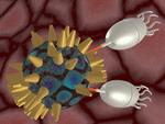

An image showing a model of BrachySil.

The scope for nanotechnology is very high as there is a lot more to explore in this field. In the subsequent articles, we will try and show you, various other perspectives nanotechnology can have. So, keep visiting us!

References: http://www.unerstandingnano.com
http://www.wikipedia.com
Article in British scientific journal, Nature.
Research paper in Forbes magazine.

MIicro Electronic Pill

By Surabhi

The invention of transistor enabled the first use of radiometry capsules, which used simple circuits for the internal study of the gastro-intestinal tract. They couldn’t be used, as they could transmit only from a single channel and also due to the size of the components. They also suffered from poor reliability, low sensitivity and short lifetimes of the devices. This led to the application of single-channel telemetry capsules for the detection of disease and abnormalities in the GI tract where restricted area prevented the use of traditional endoscopy.

They were later modified as they had the disadvantage of using laboratory type sensors such as the glass pH electrodes, resistance thermometers, etc. They were also of very large size. The later modification is similar to the above instrument but is smaller in size due to the application of existing semiconductor fabrication technologies. These technologies led to the formation of “MICROELECTRONIC PILL”.

Microelectronic pill is basically a multichannel sensor used for remote biomedical measurements using micro technology. This is used for the real-time measurement parameters such as temperature, pH, conductivity and dissolved oxygen. The sensors are fabricated using electron beam and photolithographic pattern integration and were controlled by an application specific integrated circuit (ASIC).

Continue reading

By Surabhi

Researchers in the University of Toronto’s Department of Materials Science & Engineering have developed the world’s most efficient organic light-emitting diodes (OLEDs) on plastic. This result enables a flexible form factor, not to mention a less costly, alternative to traditional OLED manufacturing, which currently relies on rigid glass.

The results are reported online in the latest issue of Nature Photonics.

OLEDs provide high-contrast and low-energy displays that are rapidly becoming the dominant technology for advanced electronic screens. They are already used in some cell phone and other smaller-scale applications.

Current state-of-the-art OLEDs are produced using heavy-metal doped glass in order to achieve high efficiency and brightness, which makes them expensive to manufacture, heavy, rigid and fragile.

“For years, the biggest excitement behind OLED technologies has been the potential to effectively produce them on flexible plastic,” says Materials Science & Engineering Professor Zheng-Hong Lu, the Canada Research Chair (Tier I) in Organic Optoelectronics.

Using plastic can substantially reduce the cost of production, while providing designers with a more durable and flexible material to use in their products.

Continue reading

By Surabhi

In a recent development, it has been found that, Smaller and more energy-efficient electronic chips could be made using molybdenite. In an article appearing online on January 30 in the journal Nature Nanotechnology, EPFL’s (Ecole polytechnique fédérale de Lausanne) Laboratory of Nanoscale Electronics and Structures (LANES) published a study showing that this material has distinct advantages over traditional silicon or graphene for use in electronics applications.

A discovery made at EPFL could play an important role in electronics, allowing us to make transistors that are smaller and more energy efficient. Research carried out in the Laboratory of Nanoscale Electronics and Structures (LANES) has revealed that molybdenite, or MoS2, is a very effective semiconductor. This mineral, which is abundant in nature, is often used as an element in steel alloys or as an additive in lubricants. But it had not yet been extensively studied for use in electronics.

100,000 times less energy

Continue reading

By Surabhi

Spiders are very agile, and some can even jump. They owe this capability to their hydraulically operated limbs. Researchers have now designed a mobile robot modeled on the same principle that moves spider legs. Created using a 3-D printing process, this lightweight can explore terrain that is beyond human reach..

Enviably agile and purposeful, the mobile robot makes its way through grounds rendered off-limits to humans as the result of a chemical accident. Depressions, ruts and other obstacles is no match for this eight-legged high-tech journeyman.

Its mission: With a camera and measurement equipment on board, it will provide emergency responders with an image of the situation on the ground, along with any data about poisonous substances. Not an easy task; after all, it must be prevented from tipping over. But this risk seems a minor one as it confidently and reliably picks its way through the area. As a real spider would, it keeps four legs on the ground at all times while the other four turn and ready themselves for the next step. Even in its appearance, this artificial articulate creature resembles an octopod. And no wonder – the natural specimen provided the model for researchers at the Fraunhofer Institute for Manufacturing Engineering and Automation IPA. This high-tech assistant is still a prototype, but future plans envision its use as an exploratory tool in environments that are too hazardous for humans, or too difficult to get to. After natural catastrophes and industrial or reactor accidents, or in fire department sorties, it can help responders, for instance by broadcasting live images or tracking down hazards or leaking gas.

Continue reading

Copper nanowires may be coming to a little screen near you. These new nano-structures have the potential to drive down the costs of displaying information on cell phones, e-readers and I Pads, and they could also help engineers build foldable electronics and improved solar cells, according to new research.

Continue reading

Scientists at London’s Imperial College have successfully managed to demonstrate digital circuits made from bacteria and DNA.

They are the most advanced biological logic gates ever created, claims the university.

“We have demonstrated that we can replicate these parts using bacteria and DNA, we hope that our work could lead to a new generation of biological processors, whose applications in information processing could be as important as their electronic equivalents,” said Professor Richard Kitney from Imperial’s Centre for Synthetic Biology.

Continue reading